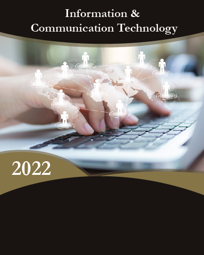
Wafer level packaging (WLP) is a technology of packaging an integrated circuit where most or all of the packaging process steps are carried out at the wafer level in contrast to the conventional chip scale packaging and wire bonding. The advancements in wafer level packaging deliver highly efficient and reliable electrical interconnect solutions for electronic products. The market holds a great potential in electronics and IT & telecommunication industries. The leading electronic companies like Samsung, Intel and Apple incorporate these packages in their products. For instance, Apple is going to incorporate wafer level fan-out package for their next generation-iPhone 7. Therefore, the increased adoption of advance packaging technology in portable electronics is expected to propel the demand of wafer level packaging in the years to come.
Roadmap for advancements in packaging technology
Wafer level packaging is a cost-effective technology with technological improvements such as lower form factor, smaller thickness, lower pitches, high density of I/O counts, lower power consumption, and higher package density, which makes it an excellent packaging technology for high end electronic gadgets. It is extensively used in portable electronic devices as it enhances the performance and durability of the device, for instance, iPhone 5 has at least 11 different WLPs, the Samsung Galaxy S3 has 6 WLPs and the HTC One X has 7. Continuous research & development activities to develop innovative and improved packaging technology, are in progress which will lead to the growth of the market.
The growing demand of wafer level packaging technology in industries such as electronics, IT & telecommunication and automotive among others would help in the growth of the wafer level packaging market. WLP enables high functionality with least cost when dealing with complex integrated circuits (IC) with a high number of input/output connections to the outside world. However, strong transmission of mechanical stress between package & board as compared to other package technologies and difficulty in repair due to restricted visual inspection hinders the growth of the market.
Wafer level packaging market is driven by trending Internet of Things (IoT), technological superiority over traditional packaging techniques and impending need of circuit miniaturization in microelectronic devices. In addition, encapsulation being a challenge for fan-out wafer level packaging and high initial investment, functions as key constraints to the market.
The market is segmented on the basis of integration type, packaging technology, bumping technology, industry vertical, and geography. Based on integration type, it is divided into fan-in WLP and fan-out WLP. The market by packaging technology comprises 3D TSV WLP, 2.5D TSV WLP, WLCSP, Nano WLP and others. Based on bumping technology, it is segmented into copper pillar, solder bumping, gold bumping, and others. The market by industry vertical comprises of electronics, IT & telecommunication, industrial, automotive, aerospace & defense, healthcare, and others. Further, the market is analyzed on the basis of regions such as North America, Europe, Asia-Pacific, and LAMEA.
Key players profiled in this report are Amkor Technology Inc., Fujitsu Ltd., Jiangsu Changjiang Electronics Technology Co. Ltd., Deca Technologies, Qualcomm Inc., Toshiba Corp., Tokyo Electron Ltd., Applied Materials, Inc., ASML Holding NV, and Lam Research Corp. among others.
POTENTIAL BENEFITS FOR STAKEHOLDERS:
This report provides an in-depth analysis of the world wafer level packaging market and offers current and future trends to identify lucrative investment pockets
This report identifies the key drivers, opportunities, and restraints that shape the market and provides an impact analysis for the forecast period
Porter's Five Forces analysis highlights the potency of buyers and suppliers that participate in this market. This would further offer a competitive advantage to stakeholders to make profitable business decisions; thereby, helping them to strengthen their supplier and buyer networks
Current and future trends are outlined to determine the overall attractiveness and highlight the profitable trends to gain a stronger foothold
Market estimation of geographic segments is derived from the current scenario and expected trends
MARKET SEGMENTATION
The market is segmented on the basis of integration type, packaging technology, bumping technology, industry vertical, and geography.
BY INTEGRATION TYPE
Fan-in WLP
Fan-out WLP
BY PACKAGING TECHNOLOGY
3D TSV WLP
2.5D TSV WLP
WLCSP
Nano WLP
Others ( 2D TSV WLP and Compliant WLP)
BY BUMPING TECHNOLOGY
Copper Pillar
Solder Bumping
Gold Bumping
Others (Aluminum & Conductive Polymer Bumping)
BY INDUSTRY
Electronics
IT & Telecommunication
Industrial
Automotive
Aerospace & Defense
Healthcare
Others (Media & Entertainment and Non-Conventional Energy Resources)
BY GEOGRAPHY
North America
U.S.
Canada
Mexico
Europe
Germany
UK
France
Netherland
Italy
Rest of Europe
Asia-Pacific
China
India
Japan
South Korea
Taiwan
Rest of Asia-Pacific
LAMEA
Latin America
Middle East
Africa
KEY PLAYERS
Amkor Technology Inc.
Fujitsu Ltd.
Jiangsu Changjiang Electronics Technology Co. Ltd.
Deca Technologies
Qualcomm Inc.
Toshiba Corp.
Tokyo Electron Ltd.
Applied Materials, Inc.
ASML Holding NV
Lam Research Corp.